ECE216 | Exp2 | Analysis and Synthesis of Arithmetic Expressions using Adders/Subtractors

CoderIndeed
0

Introduction

About the Experiment

  • This experiment enables a student to learn
  • How to realize the functionality of IC 7483, a 4 bit binary full adder
  • How to realize the functionality of 8 bit full adder by carcading two 7483 chips(two 4 bit full adder)
  • how to implement a 4 bit adder/substractor.

Theory

Part I

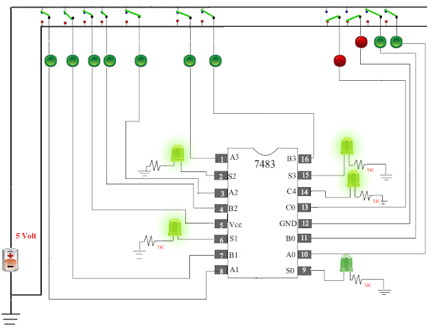
IC 7483 is 4-bit binary full adder which accepts two 4-bit binary words A3A2A1A0 and B3B2B1B0 and a carry input (C0) as inputs and produces a 4-bit binary sum output S3S2S1S0 and a carry output C4.

Figure1

The students of virtual DEC Laboratory can verify the functionality of the 7483 chip.Although in principle,there can be 29=512 input paterns possible,the students can verify all zero,all one and some other patterns.

Part II

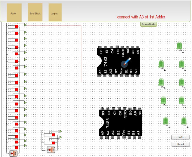
Cascading of two 7483 chips to achieve addition of two 8-bit numbers A = A8A7A6A5A4A3A2A1 and B = B8B7B6B5B4B3B2B1 to produce Sum = S8S7S6S5S4S3S2S1 and carry output C9 of the 217 input patterns possible , the students can test the 8bit adder for all zeros , all ones and some other input patterns.


Figure 2(i)

Figure 2(ii)


Part III

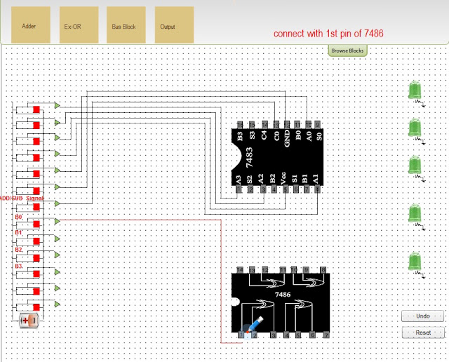
To implement a 4 bit adder/subtractor using 2's complement number system.Students learnt the use of 7486 (qued 2-input Ex-OR gates)in experiment 3.Using a 7483(parallel adder) and a 7486 chip one can realize 4 bit adder/subtractor.If ADD/SUB = "0" normal addition S = A + B performed.On the other hand if ADD/SUB = "1" then S = A + [B] + 1 where [B] = 1's complement of B. For example,if A = 0111(7) and B = 0101(5) then [B] = 1010 and S = 0010 or 2 neglecting carry out C4.If however A = 0101(5) and B = 0111(7) then B = 1000; or S = 1110 which represents -2 in 2's complement number system.


Objective

Aim of the Experiment

The objective of part 1 of the experiment is to fully understand the functionality of 4 bit binary full adder.
The objective of part 2 of the experiment is to fully understand the functionality of 8 bit full adder by carcading to 7483 chips(two 4 bit full adder).
The objective of part 3 of the experiment is to fully understand the functiponality and implementation of 4 bit adder/subtractor.

Procedure

Please follow these steps to do the experiment.

Please follow these steps to do the experiment(Part-I)


1. At first click on the Vcc switch that means Vcc = 1 and GND = 0 , show message Vcc & GND properly connected.


2.  Next, A0= 1, A1= 0, A2= 0, A3= 0 and B0= 1, B1= 0, B2= 0, B3= 0 now you can see the output result of S0= 0, S1= 1, S2= 0, S3= 0 and C4= 0.


3.  Next, A0= 0, A1= 0, A2= 0, A3= 0 and B0= 1, B1= 1, B2= 0, B3= 0 now you can see the output result of S0= 1, S1= 1, S2= 0, S3= 0 and C4= 0.


4.  Next, A0= 0, A1= 0, A2= 0, A3= 1 and B0= 0, B1= 0, B2= 0, B3= 1 now you can see the output result of S0= 0, S1= 0, S2= 0, S3= 0 and C4= 1.


5.  Next, A0= 1, A1= 1, A2= 1, A3= 1 and B0= 1, B1= 1, B2= 1, B3= 1 now you can see the output result of S0= 0, S1= 1, S2= 1, S3= 1 and C4= 1.


Please follow these steps to do the experiment(Part-II)


1.  At first click on the Browse Block button
2.  Next, drag the Adder block and drop it onto the bread board.


3.  Next, drag the Bus block and drop it onto the bread board.


4.  Next, drag the output block and drop it onto the bread board.


5.  Next, make a connection from switch A to A3 of the 1st Adder..


6.  Next, make a connection from C4 of the 1st Adder to C0 input of the 2nd Adder..


7.  Next, make a connection from switch L to A3 of the 2nd Adder...


8.  Next, make a connection from S0 of 1st Adder to 3rd LED...


9.  Overall connection...


10.  Switch on the Vcc of the 1st & 2nd Adder & switch on the A0 & B0 of 1st Adder..


11.  Switch on the Vcc of the 1st & 2nd Adder & switch on the A0,A1,A2,A3 & B0,B1,B2,B3 of 1st Adder and switch on the A0,A1,A2,A3 & B0,B1,B2,B3 of 2nd Adder ..


12.  Switch on the Vcc of the 1st & 2nd Adder & switch on the A0,A1,A2,A3 & B0,B1,B2,B3 of 2nd Adder ..


13.  Switch on the Vcc of the 1st & 2nd Adder & switch on the A0,A1,A2,A3 & B0,B1,B2,B3 of 1st Adder ..


Please follow these steps to do the experiment(Part-III)


1.  At first click on the Browse Block button
2.  Next, drag the Adder block and drop it onto the bread board.
3.  Next, drag the Ex-OR-Gate block and drop it onto the bread board.


4.  Next, drag the Bus block and drop it onto the bread board.


5.  Next, drag the output block and drop it onto the bread board.
6.  Next, make a connection from switch A to A3 of the Adder..


7.  Next, make a connection from switch H to 1st pin of 7486.


8.  Next, make a connection from C0 of Adder to 2nd pin of 7486.


9.  Next, make a connection from 2nd pin of 7486 to 5th pin of 7486.
10.  Next, make a connection from 5th pin of 7486 to 9th pin of 7486.
11.  Next, make a connection from 9th pin of 7486 to 12th pin of 7486.


12.  Next, make a connection from 11th pin of 7486 to B3 of Adder.
13.  Next, make a connection from 8th pin of 7486 to B2 of Adder.


13.  Next, make a connection from 3rd pin of 7486 to B0 of Adder.
14.  Next, make a connection from 6th pin of 7486 to B1 of Adder.


15.  Next, make a connection from S1 of Adder to 2nd LED...


16.  Next, switch on the Vcc of Adder & 14th pin of 7486(for Vcc) and switch on the ADD/SUB then switch on the A0,A1,A2 of Adder & switch on the B0,B2 of 7486.


17.  Next, switch on the Vcc of Adder & 14th pin of 7486(for Vcc) and switch on the ADD/SUB then switch on the A0,A2 of Adder & switch on the B0,B1,B2 of 7486.


18.  Next, switch on the Vcc of Adder & 14th pin of 7486(for Vcc) and switch off the ADD/SUB then switch on the A0,A1,A2,A3 of Adder & switch on the B0,B1,B2,B3 of 7486.


19.  Next, switch on the Vcc of Adder & 14th pin of 7486(for Vcc) and switch off the ADD/SUB then switch off the A0,A1,A2,A3 of Adder & switch on the B0 of 7486.

Tags

Post a Comment

0Comments

Post a Comment (0)

#buttons=(Accept !) #days=(20)

Our website uses cookies to enhance your experience. Check Now
Accept !